| quad VCO |
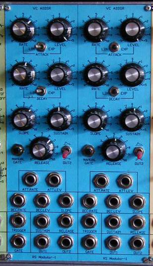
| dual VC ADDSR |
| dual VCF |
| dual VCA |
| modulator |
| divider |
| mixer |
| sequencer |
| S&H |
| power supply |
| keyboard |
| MIDI2CV |
| SOUNDS |
|
This envelope generator was the first thing which came into my mind when I decided to make a nice modular synth,
but it took me more than I expected to finish it. I couldn't resist to make it 5 stages, bipolar and voltage controlled.
ADDSR stands for Attack, Decay 1, Decay 2, Sustain, Release. Maybe I should name it ADBDSR (decay-break-decay).
Originally it ought to have voltage controlled "punch" (transition from linear to log slope) in attack and 1st
decay stage. Unfortunately nonlinearities in control paths (don't ask) killed this idea. It is completely tested, working circuit, but I may introduce some changes later. Any comments are appreciated.
Specifications
|
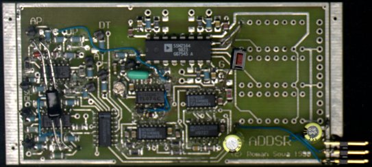
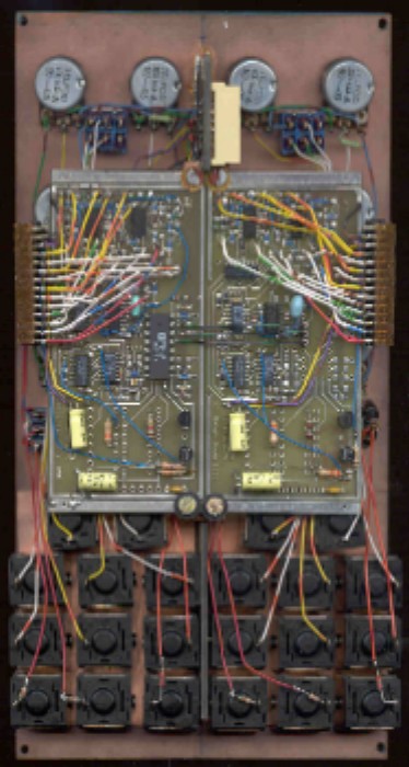
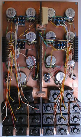
see the back of it, and the back without the boards |
Schematic and techtalk
 Click on the image to see large, readable schematic |
- Attack GATE goes high. D-flops get reset. Gates U6A&B generate address 01 for analog mux which routes attack level voltage as base voltage for integrator, and "attack time" control voltage (via inverting amplifier U8B) to VCA control input. Base voltage is always greater (with respect to GND) than applied control voltage - that's why U7B. Normally "lin att" switch is open and the difference is small, hence we get log attack slope. When "lin att" is closed, the voltage applied to integrator is 2.5 times greater than attack peek level and it works in almost linear region of exp. charging curve. The result is "linear" attack slope. The same could be done to first decay. The integrator is charging C7. When output voltage reaches attack level (note that voltages at comparator inputs are inverted and attenuated by ratio 5:3), the comparator U2B toggles (R26 and R30 give little hysteresis) and sets U4A D-flop. Those circuits between comparators and D-flops make trigger pulse every time comparator toggles.
- First decay. So now we have U4A set, and the mux address is 00. Decay peek (or break) voltage is applied as base, and "decay time" as VCA control. When integrator voltage reaches decay level, second comparator (U2A) toggles. Possible toggles of attack comparator don't matter, because U4A is already set, and decay comparator toggles could not have any effect before attack stage finished (D input of U4B was 0). The mux address gets to 10.
- Second decay and sustain With mux address 10 integrator discharges to sustain level with rate set by "sustain time" control voltage (I use the name "sustain time" for "second decay time" - I know it is misleading). Now the base voltage is routed directly (via inverter, but still..) to integrator and it discharges to sustain level exponentially. Nothing else changes while GATE is on.
- Release GATE goes low. Logic generates address 11 for mux, and integrator discharges to 0V with rate set by "release time" control. Release time is selected every time GATE goes low, no matter in what stage EG was at the time.
Most important parts
- VCA:
- I used 1/4 of SSM2164 with intention to use other 3 as modulation VCAs. It could be any other OTA or discrete VCA. Beware of offset voltage though...
- logic:
- 4011 gate, 4013 D-flop, 4052 dual mux - powered from 18V (!)
- opamps:
- TL074; any opamp will do, only integrator should be low input bias current.
- resistors:
- R25 sets envelope time boundaries
- R20 sets envelope time range
- R7 set decay slope curve; use smaller for more linear and bigger for more log
- (R14=R3=R5=R1=R11) =5/3* (R35=R4=R6=R2=R12) unless linear attack is not needed - then all those resistors must be equal.